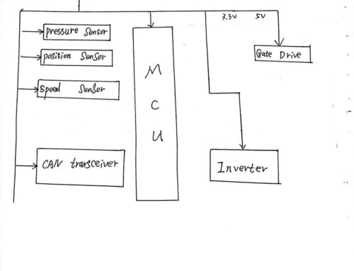
What is the Electronic Chip Package
Electronic Chip Package means that the circuit pins on the silicon chip which used for connected to the external connectors by wires to connect with other devices. The package form refers as the case for mounting semiconductor integrated circuit chips. It not only functions to install, fix, seal, protect the chip and enhance the electric thermal performance, but also use wires connects to the pins of the package case by connect point of the chip, and these pins pass through the wires on the printed circuit board connected to other devices,so that internal chip can connected to external circuits. Because the chip must be isolated from the outside world to prevent corrosion of the chip circuit by impurities in the air cause the electrical performance is degraded. On the other hand, the packaged chip is also easier to install and transport. It is crucial because the quality of the packaging technology directly affects the performance of the chip itself and the design and manufacture of the PCB (printed circuit board) which connected to the chip.
An important indicator to measure the advancement of a chip packaging technology is the ratio of chip area to package area. The ratio is closer to 1 and the better. The main factors to consider when packaging:
1, the ratio of chip area to package area is to improve packaging efficiency, as close as possible to 1:1;
2, the pin should be as short as possible to reduce the delay, the distance between the pins as far as possible to ensure no mutual interference, and improve performance;
3. Based on the requirements of heat dissipation, the thinner the package, the better.
The package is mainly divided into DIP dual in-line and SMD two package. In terms of structure, the package experienced the earliest transistor TO (such as TO-89, TO92) package and developed into a dual in-line package. Subsequently, PHILIP developed a small SOP package, and later derived SOJ (J type Pin small outline package), TSOP (thin small outline package), VSOP (very small outline package), SSOP (reduced SOP), TSSOP (thin reduced SOP) and SOT (small outline transistor), SOIC (small outline) Integrated circuit) and so on. From the material media, including metals, ceramics, plastics, plastics, there are still a lot of metal packaging for circuits that require high-intensity working conditions, such as military and aerospace.
The package has undergone the following development process:
Structural aspects: TO->DIP->PLCC->QFP->BGA->CSP;
Materials aspects: metal, ceramic -> ceramic, plastic -> plastic;
Pin shape: long lead in-line -> short lead or leadless mounting -> spherical bump;
Assembly method: through hole insertion -> surface assembly -> direct installation
Specific package form
1, SOP / SOIC package
SOP is the abbreviation of Small Outline Package, which is a small outline package. The SOP packaging technology was developed by Philips from 1968 to 1969. Later, it gradually derived SOJ (J-type small outline package), TSOP (thin small outline package), VSOP (very small outline package), SSOP (reduced type). SOP), TSSOP (Thin Reduced SOP) and SOT (Small Outline Transistor), SOIC (Small Outline Integrated Circuit), etc.
2, DIP package
DIP is the abbreviation of Double In-line Package, which is a dual in-line package. One of the plug-in packages, the leads are led out from both sides of the package, and the package materials are plastic and ceramic. DIP is the most popular plug-in package, and its application range includes standard logic IC, memory LSI, and microcomputer circuit.
3, PLCC package
PLCC is the abbreviation of Plastic Leaded Chip Carrier, which is a plastic J lead chip package. The PLCC package is square in shape, 32-pin package, and has pins around it. The external dimensions are much smaller than the DIP package. The PLCC package is suitable for mounting wiring on the PCB with SMT surface mount technology, and has the advantages of small size and high reliability.
4, TQFP package
TQFP is the abbreviation of Thin Quad Flat Package, which is a thin plastic four-corner flat package. The Quad Flat Package (TQFP) process effectively utilizes space, reducing the need for printed circuit board space. Due to the reduced height and size, this packaging process is ideal for space-critical applications such as PCMCIA cards and networking devices. Almost all ALTERA CPLD/FPGAs have a TQFP package.
5, PQFP package
PQFP is the of English Plastic Quad Flat Package, which is a plastic four-corner flat package. The PQFP package has a small distance between the chip pins and a very small pin. Generally, large-scale or very large-scale integrated circuits use this package, and the pin count is generally above 100.
6, TSOP package
TSOP is the abbreviation of Thin Small Outline Package, which is a thin and small package. A typical feature of TSOP memory packaging technology is the ability to make pins around the packaged chip. TSOP is suitable for mounting wiring on PCBs (printed circuit boards) using SMT technology (surface mount technology). In the case of the TSOP package, the parasitic parameters (when the current changes greatly, causing the output voltage to be disturbed) are reduced, which is suitable for high-frequency applications, the operation is convenient and the reliability is relatively high.
7, BGA package
BGA is the abbreviation of Ball Grid Array Package, which is a ball grid array package. With the advancement of technology in the 1990s, the integration of chips continued to increase, the number of I/O pins increased sharply, power consumption also increased, and the requirements for integrated circuit packaging were also stricter. In order to meet the needs of development, BGA packaging began to be applied to production.
The memory packaged by BGA technology can increase the memory capacity by two to three times when the memory volume is constant. Compared with TSOP, BGA has smaller volume, better heat dissipation performance and electrical performance. BGA packaging technology has greatly improved the storage capacity per square inch. The memory products with BGA packaging technology are only one-third of the TSOP package under the same capacity. In addition, compared with the traditional TSOP package, the BGA package has a faster and more efficient way to dissipate heat.
The I/O terminals of the BGA package are distributed in the form of arrays of circular or columnar solder joints under the package. The advantage of the BGA technology is that although the number of I/O pins is increased, the distance of the pins is not smaller but wider. Increased assembly yield rate; although its power consumption increases, BGA can be soldered with a controlled collapse chip method to improve its electric thermal performance; thickness and weight are reduced compared to previous packaging techniques; parasitic parameters are reduced, The signal transmission delay is small, the frequency of application is greatly improved;
When it comes to BGA packaging, it must to mention Kingmax’s patented TinyBGA technology. TinyBGA called Tiny Ball Grid Array, which is a branch of BGA packaging technology. It was developed by Kingmax in August 1998. The ratio of chip area to package area is not less than 1:1.14, which can increase the memory capacity by 2-3 times when the memory volume is constant, compared with TSOP package products. It has a smaller volume, better heat dissipation and electrical properties.
Description of the suffix:
1. In the suffix, J indicates the civilian product (0-70 ° C), N indicates the ordinary plastic seal, and R in the suffix indicates the surface sticker.
2. The suffix with D or Q indicates pottery seal, industrial grade (45°C-85°C). H in the suffix indicates a round cap.
3. SD or 883 is a military product in the suffix.For example: JN DIP package JR surface mount JD DIP pottery seal