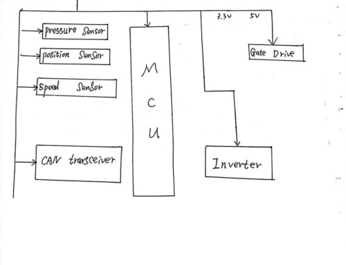
For electronic products, printed circuit board design is the absolutely necessary process from the electrical schematic diagram to a specific product. The design’s rationality very closed to the production and the product’s quality, and for many designers who just engaged in electronic design are less experience in this field, the printed circuit boards designed from them often have some problems,although them has learned the printed circuit board design software. The writer have worked for many years in the printed circuit board design work,and glad to share some experience for printed circuit board design and hope it’s useful for some PCB designers. The writer usually use the PROTEL2.7 software.
A.The sequence for components on the printed circuit board:
- Place the components which are tightly fitted with the whole structure in a fixed position, such as a power outlet, lights, switches, connectors, and so on. Use the LOCK function locked components after them placed on the board,so that they can,t moved by your mistake action.
- Place the special components on the board such as heat generating elements, transformers, ICs and so on.
- Place the small devices.
B.The distance of the component from the edge of the board: If possible, all components are placed within 3 mm from the edge of the board or at least the distance more than the thickness of the board. Because need some space for guide rails in the mass production of the assembly line and wave soldering, also can prevent defect of edge board during the processing. If need to put much components on printed circuit board, had to beyond the 3mm range, you can add the edge of the board 3mm auxiliary side, auxiliary side open V-shaped Groove, in the production can be broken by hand.
C.Isolation between high and low voltage: in many printed circuit board both have high-voltage circuit and low-voltage circuit. The components placed on high-voltage circuit part need to be separated from the low-voltage circuit part. The isolation distance depeond on the bear pressure,usually the distance is 2mm in the 2000V board, and need to increase the distance for more high Voltage board , for example, to withstand the 3000V pressure test, the distance between high and low voltage lines should be at least 3.5mm, in many cases to avoid Creeping, need to open a slot between the high and low voltage.
D.The alignment of printed circuit board :The printed lines should be as short as possible especially in the high frequency circuits; the corners of the printed line should be rounded angle,the Right angle or sharp angle may affect the electrical performance in the case of high frequency circuits and high lines densities ; When the lining the double boards,the lines of front and back should be perpendicular,oblique or bend alignment to each other,need to avoid parallel to each other to reduce the parasitic coupling; as the printed lines for input and output should try to avoid adjacent parallel, it’s better to add a ground line between these lines.
E.Width of printed lines:
Width of lines should be able to meet the electrical performance requirements and easy to produce, it’s smallest size depend on the current, but the minimum should not be less than 0.2mm, in high-density, high-precision printed circuit, the line width usually is 0.3mm; When decide the line width also consider its temperature rise in the case of high current. The experiments of single boards show that when the copper thickness is 50μm, the line width as 1 ~ 1.5mm, through the current 2A, the temperature rise is very small, therefore, generally use 1 ~ 1.5mm width line may meet the design requirements and would no causing temperature rise; The public ground line should be as thick as possible, if possible, use lines greater than 2 to 3 mm, this is very important in circuits which with the microprocessors,because if the local line too thin would due to changes of current in the ground potential, and the microprocessor timing signal instability, would make the noise margin degradation; in the DIP package for IC between the lines, can use the 10-10 and the 12-12 principle, that is, when two lines through between two feet, the pad diameter can be set as 50mil, line width and line spacing as 10mil, when only one line through the two feet, the pad diameter can be set to 64mil, line width and line spacing can be 12mil.
F.Printed line spacing:The space between Adjacent conductors must meet electrical safety requirements, and easy for operation and production, the spacing should be as wide as possible. The minimum spacing at least can be able to withstand the voltage. This voltage typically includes the operating voltage, the additional ripple voltage, and the pera voltage caused by other reasons. When the printed lines density is low, the space between the signal lines can be increased appropriately, and for the signal lines of the high and low levels should be as short as possible and add increase the space
G.Ground lines and shield function :
Public ground line should be arranged in the edge of the board. Should retain the copper foil as much as possible in the PCB board to do the ground line, can get the better shielding effect compare with the long ground line, transmission line and shielding effect will be improved, and can reduce the distribution of capacitance. The The common ground line of printed lines is preferably looped or reticulated,because when there are many integrated circuits on the same board, especially when there are many power consuming components,the limitations of pcb figure make the Potential difference, resulting in reduced noise margin, when made into a loop, the ground potential difference decreases.
H.Sold Pad:
The diameter the inner size of the pad: the inner hole size usully no less than 0.6mm,it hard to process when open the mould if the inner hole size less than 0.6mm,the diameter of pad usually add 0.2mm on the basis of diameter of the components feet. For example if the diamater of resistance’s feet pin is 0.5mm.then the inner size of the pad is 0.7mm.